Research Area
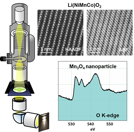
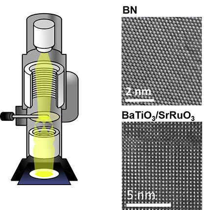
Atomic resolutionSTEM & EELS
High resolutionTEM image
Convergent beam & nano beam electron diffraction
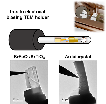
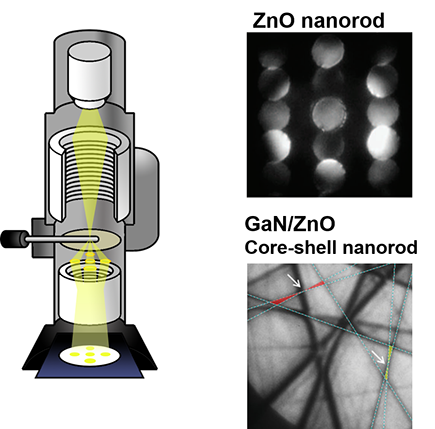
In-situ TEM
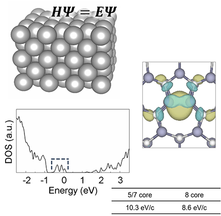
DFT caculation
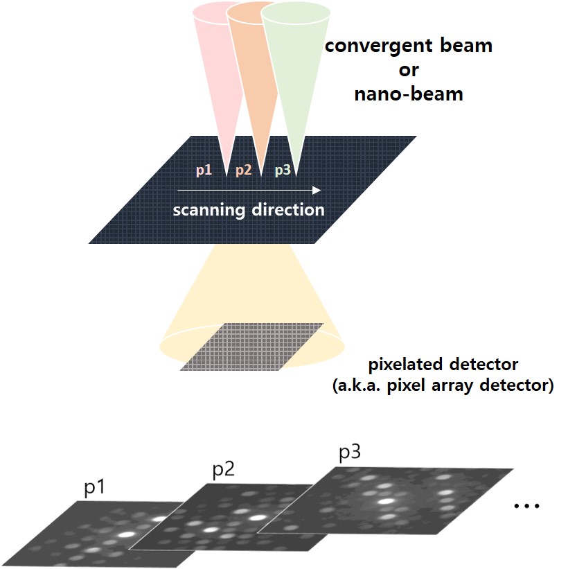
4-dimensional STEM
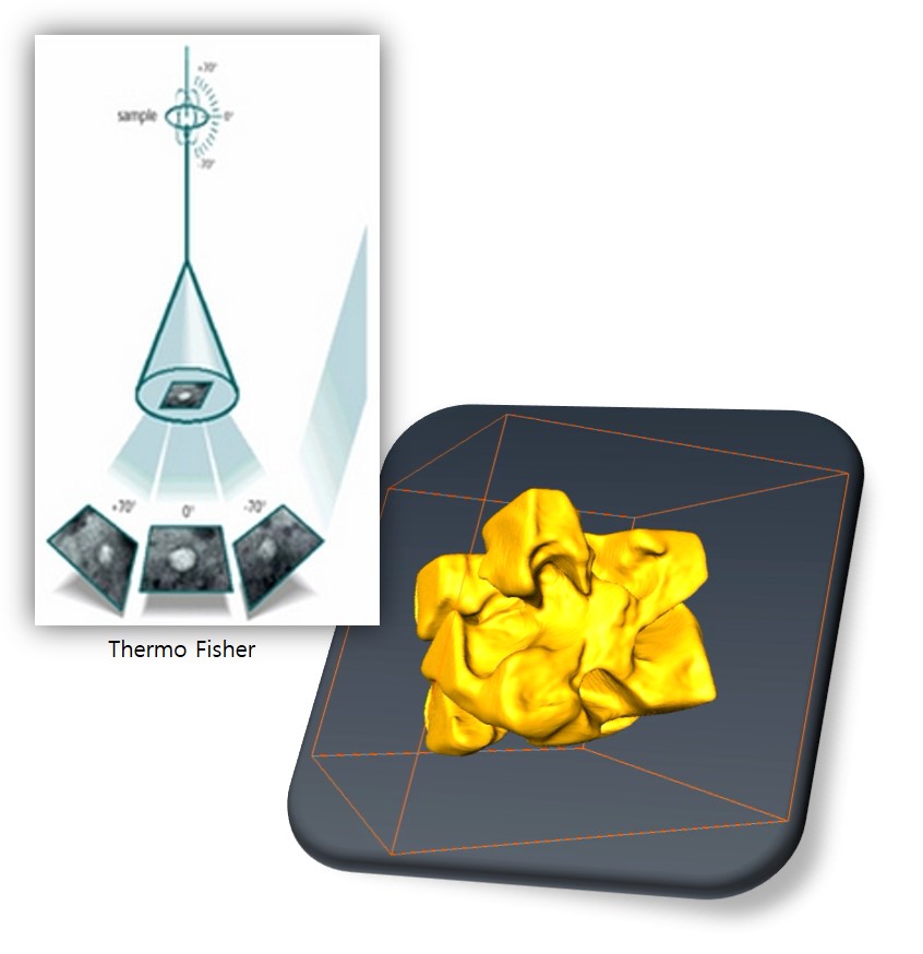
Electron Tomography (S/TEM, EDS, EELS)
The primary goal of our research is to understand the structure-property relationship in advanced materials, for which we utilize several advanced TEM-related techniques including atomic-resolution STEM/EELS, CBED, electron holography or in-situ electrical biasing experiment. Furthermore, we try to correlate atomic and electronic structures of advanced materials with their physical properties using DFT calculations. Our group members are trained to be experts in the characterization of advanced materials. We believe that our research further leads to design functional materials or devices of new concept.
Covers